

HomeCoursesMTech in Electronics & Communication (VLSI Design / Communication System)
PGEngineering & Technology

MTech in Electronics & Communication (VLSI Design / Communication System)

MTech in Electronics & Communication (VLSI Design / Communication System) is a 2-year full-time postgraduate programme taught on the MIT University Sikkim campus at Namchi, Sikkim, across 4 semesters and 80 credits (Level 7). Electronics & Communication (VLSI Design / Communication System) is the main subject in every year, supported by practical work, a project or internship and continuous assessment. Eligibility: Btech in Relevant Subject. On completion the award is MTech — 80 Credits (2-Year PG).

Duration
2 yrs
Approval
UGC Recognised
Eligibility
Btech in Relevant Subject
Mode
Regular
NEP 2020 logo
NEP 2020
UGC Approved logo
UGC Approved
AIU Member logo
AIU Member
Sikkim Government logo
Sikkim Government
MOE logo
MOE
Course Overview

About MTech in Electronics & Communication (VLSI Design / Communication System) Course

MTech in Electronics & Communication (VLSI Design / Communication System) at MIT University Sikkim takes 2 years and focuses on how technical systems and structures are designed, tested and maintained safely, taught as a regular on-campus programme.

Alongside the Electronics & Communication (VLSI Design / Communication System) papers you get workshop and laboratory sessions, drawing and CAD practice and measurement and testing exercises. The award on completion is MTech, and the work you produce during the programme becomes your portfolio.

What MTech in Electronics & Communication (VLSI Design / Communication System) gives you

  • A single clear subject focus: Electronics & Communication (VLSI Design / Communication System), studied properly for 2 years rather than spread thin.
  • Practical work every semester — workshop and laboratory sessions, drawing and CAD practice and measurement and testing exercises — so you can show what you can do, not only what you studied.
  • Subject choices that stay relevant: Electronics & Communication (VLSI Design / Communication System): Advanced Theory & Practice, Electronics & Communication (VLSI Design / Communication System): Applied / Industry Track and Electronics & Communication (VLSI Design / Communication System): Research & Analytics Track.
  • A degree from a UGC-recognised state private university, valid for employment and for further study.
  • Small campus, direct access to faculty, and daily classroom support at Namchi, Sikkim.

What you will be able to do

  • Read and prepare technical drawings in the context of Electronics & Communication (VLSI Design / Communication System).
  • Apply standard testing and quality procedures in the context of Electronics & Communication (VLSI Design / Communication System).
  • Use core engineering software tools in the context of Electronics & Communication (VLSI Design / Communication System).
  • Work safely to documented procedure in the context of Electronics & Communication (VLSI Design / Communication System).
  • Complete an independent Electronics & Communication (VLSI Design / Communication System) dissertation from question to final defence.
UGC-recognised university

MIT University Sikkim is a state private university established by the Government of Sikkim under Sikkim Act No. 11 of 2024. MTech in Electronics & Communication (VLSI Design / Communication System) is taught as a regular university programme.

Faculty access

Batch sizes stay small enough that Electronics & Communication (VLSI Design / Communication System) faculty know each student, review project work individually and are reachable outside class hours.

Learning environment

A quiet Himalayan campus with residential facilities, sport and student activities — useful for a programme like MTech in Electronics & Communication (VLSI Design / Communication System) that needs consistent daily study.

Career preparation

Resume writing, communication and interview practice are part of the programme, aimed at the roles MTech in Electronics & Communication (VLSI Design / Communication System) graduates actually apply for.

Course Guide

MTech in Electronics & Communication (VLSI Design / Communication System) — Complete Course Information

1Programme Structure & Credit System

MTech in Electronics & Communication (VLSI Design / Communication System) is a 2-year, 80-credit postgraduate programme taught full-time on the Namchi campus across 4 semesters at Level 7, under NEP 2020 and the Choice Based Credit System.

You study single subject (1), with electives such as Electronics & Communication (VLSI Design / Communication System): Advanced Theory & Practice, Electronics & Communication (VLSI Design / Communication System): Applied / Industry Track and Electronics & Communication (VLSI Design / Communication System): Research & Analytics Track, research methodology and a dissertation or major project leading to MTech — 80 Credits (2-Year PG).


2Eligibility & Who Should Apply

The minimum qualification is Btech in Relevant Subject. Admission is merit based, with no entrance examination and no upper age limit.

The programme suits students aiming at a career in engineering & technology, working candidates who need a recognised degree, and anyone planning higher studies or competitive examinations.

3Curriculum & What You Will Learn

The early semesters build the foundation of Electronics & Communication (VLSI Design / Communication System) alongside language, digital and multidisciplinary courses; the middle semesters move into core theory and applied work in areas such as Electronics & Communication (VLSI Design / Communication System): Advanced Theory & Practice, Electronics & Communication (VLSI Design / Communication System): Applied / Industry Track, Electronics & Communication (VLSI Design / Communication System): Research & Analytics Track and Electronics & Communication (VLSI Design / Communication System): Contemporary Issues.

The final year adds advanced coursework, an internship or on-the-job training and a dissertation, with continuous internal assessment and built-in soft-skill, resume and interview training.

4Career Opportunities & Higher Studies

Graduates typically start in roles such as Site Engineer, Design Engineer, Maintenance Engineer and Quality Engineer, in both private organisations and government recruitment where the notification allows.

The qualification supports admission to research and doctoral programmes and is widely accepted for teaching-eligibility examinations in the discipline.

5Admission Process for 2026

Apply online on the official portal: fill in your personal and academic details, upload documents and pay the ₹10,000 registration fee. Applications for the 2026 session are open now.

The admissions team verifies your documents and confirms eligibility, usually within a couple of working days, after which you complete the fee formalities and receive your enrolment number. Counselling is free — call +91 6009466009 or submit the enquiry form on this page.

6Fees, Scholarships & Required Documents

Fees vary by programme and year of entry; the current structure is shared by the admissions team and the official fee document is available on the downloads page. Eligible students may receive a scholarship or fee benefit, and 25% of seats are reserved for eligible Sikkim-domicile students.

Keep scanned copies ready: Class 10 and 12 marksheets and certificates, graduation marksheets and provisional or degree certificate, transfer or migration certificate where applicable, a government photo ID such as Aadhaar, a passport-size photograph, your signature, and a category or domicile certificate if claiming a reserved seat or scholarship.

Approval & Recognition

Is MTech in Electronics & Communication (VLSI Design / Communication System) a Valid Degree?

Yes. MTech in Electronics & Communication (VLSI Design / Communication System) is awarded by MIT University Sikkim. Approval reference: UGC | MOE | Government of Sikkim approved university programme.

  • UGC | MOE | Sikkim Government approved university programme
  • MIT University Sikkim is a state private university established by the Government of Sikkim
  • Regular-mode study follows university assessment rules, assignments, examinations, practicals, projects or viva where applicable
  • The qualification may be used for jobs, higher education and competitive exams subject to the rules of the recruiting or admitting authority

Students should verify the latest recognition, mode approvals and examination rules from the university before admission.

Limited Seats Available

Ready to Start Your MTech in Electronics & Communication (VLSI Design / Communication System) Journey?

Take the next step today, our counsellors respond within 30 minutes.

At a Glance

MTech in Electronics & Communication (VLSI Design / Communication System) Course Highlights

Duration
2 Years
4 Semesters
Degree Level
PG
Full-time programme
Study Mode
Regular
On-campus, full time
Approval
UGC
Govt. of Sikkim established
Course NameMTech in Electronics & Communication (VLSI Design / Communication System)
Degree LevelPG
Duration2 Years (4 Semesters)
ModeRegular (Full-time, on-campus at Namchi)
ApprovalUGC (University Grants Commission) Approved
EligibilityBtech in Relevant Subject
Admission ProcessMerit-based · 100% online application · Document verification · No entrance exam
Core SubjectsElectronics & Communication (VLSI Design / Communication System): Advanced Theory & Practice · Electronics & Communication (VLSI Design / Communication System): Applied / Industry Track · Electronics & Communication (VLSI Design / Communication System): Research & Analytics Track · Electronics & Communication (VLSI Design / Communication System): Contemporary Issues
Skills You'll LearnCritical thinking · Communication · Analytical reasoning · Electronics & Communication (VLSI Design / Communication System) domain expertise
Career OpportunitiesSite Engineer · Design Engineer · Maintenance Engineer · Quality Engineer
Government Job EligibilityYes, subject to the recruiting authority's eligibility criteria
Private Job EligibilityYes
Credits80 credits · Level 7
University RecognitionMIT University, Sikkim, UGC approved & established by the Government of Sikkim

Swipe left/right to view the full table.

Why This Course

Why Choose MTech in Electronics & Communication (VLSI Design / Communication System)?

Reason 01

Updated syllabus covering Electronics & Communication (VLSI Design / Communication System): Advanced Theory & Practice as per current industry demand

Reason 02

Placement assistance for roles such as Site Engineer, Design Engineer, Maintenance Engineer

Reason 03

Practical work in every semester — workshop and laboratory sessions and drawing and CAD practice

Reason 04

Free 30-minute career counselling before admission to choose the right path

Reason 05

UGC | MOE | Sikkim Government approved and valid for jobs and higher studies

Reason 06

Regular mode study with experienced faculty and daily classroom support

Recognised · Approved · Trusted

Degree Validity & Recognition

Govt. of Sikkim

Established by State Act

UGC

Recognized University

NIRF

Participating in Rankings

NEP 2020

CBCS Structure

Your Degree is 100% Valid

Regular Degree — same value as any on-campus degree
Valid across Delhi & all India for jobs & studies
Accepted for Higher Education (PhD, PG, etc.)
Eligible for Government Jobs (as per recruitment rules)
Accepted by Private Companies nationwide
Useful for UGC NET & competitive exams

Key Student Benefits

UGC-Compliant Degree

Recognized qualification valid for jobs, promotions, and higher studies across India.

Industry-Oriented Curriculum

Practical, skill-based learning with internships built into many programs.

NEP 2020 & CBCS

Modern credit-based structure that matches national education standards.

Affordable Fees + Scholarships

5% merit scholarships for economically weaker students, plus flexible EMI.

Limited Seats Available

Ready to Start Your MTech in Electronics & Communication (VLSI Design / Communication System) Journey?

Take the next step today, our counsellors respond within 30 minutes.

How You Study

Study Mode: Regular (On-Campus)

Regular Mode

Full-time on-campus study at Namchi, Sikkim with daily classes, practicals, library access, seminars and campus life. Best for students who want the complete university experience.

What a week looks like

Electronics & Communication (VLSI Design / Communication System) lectures and tutorials, scheduled practical sessions, and continuous internal assessment through the semester. Attendance, examinations and project submission follow the university academic calendar.

Explore all programmes
Who Can Apply

Eligibility Criteria & Duration

Qualification
Btech in Relevant Subject
Duration
2 Years
Age Limit
No upper limit
Credits
80 Credits

Eligibility for MTech in Electronics & Communication (VLSI Design / Communication System)

  • Minimum qualification for MTech in Electronics & Communication (VLSI Design / Communication System): Btech in Relevant Subject, from a recognised board or university.
  • The qualifying degree should be in Electronics & Communication (VLSI Design / Communication System) or a closely related science discipline, with the relevant subject studied at graduation level.
  • Minimum aggregate marks in the qualifying degree as per the University's admission norms; relaxation for reserved categories as per applicable rules.
  • Admission is merit-based — no entrance examination and no upper age limit.
  • The award on completion is MTech — 80 Credits (2-Year PG), issued by MIT University Sikkim as a UGC-recognised state private university.

Duration

2 Years · 4 Semesters (CBCS / NEP 2020)

  • Year 1: Foundation of Electronics & Communication (VLSI Design / Communication System), Electronics & Communication (VLSI Design / Communication System): Advanced Theory & Practice, Research Methodology
  • Year 2: Advanced Electronics & Communication (VLSI Design / Communication System), Industry Internship / On-Job Training, Dissertation / Research Project

Note: Eligibility may vary from course to course and is subject to change as per the latest MIT University Sikkim admission rules, UGC guidelines and NEP 2020 provisions. Students are advised to verify course-specific eligibility with the University Admission Cell or an authorised Education Counsellor before applying — call +91 6009466009 or submit the enquiry form on this page.

Limited Seats Available

Ready to Start Your MTech in Electronics & Communication (VLSI Design / Communication System) Journey?

Take the next step today, our counsellors respond within 30 minutes.

How to Apply

Admission Process 2026

100% Online
No entrance exam
30-Min Callback
Free counselling
Merit-Based
Direct admission
  1. 01
    Step 1

    Fill the online enquiry / application form for the 2026 session

  2. 02
    Step 2

    Free counselling call — eligibility and specialisation check within 30 minutes

  3. 03
    Step 3

    Upload documents (marksheets, ID proof, photograph) for verification

  4. 04
    Step 4

    Pay the ₹5,000 registration fee to block your seat

  5. 05
    Step 5

    Receive the provisional admission letter and enrolment number

  6. 06
    Step 6

    Pay the first-year fee (full or instalment) to confirm admission

  7. 07
    Step 7

    Classes begin — LMS/ID card, timetable and student support activated

Documents Checklist

Keep scanned copies ready
  1. Document 01
    10th marksheet
  2. Document 02
    12th marksheet
  3. Document 03
    Graduation marksheet (for PG)
  4. Document 04
    Transfer / migration certificate
  5. Document 05
    ID proof (Aadhaar / Passport)
  6. Document 06
    Passport-size photographs

Documents required: 10th & 12th marksheets, graduation marksheet (for PG), transfer/migration certificate, ID proof and passport-size photographs.

Admission 2026

Admission Guidance for MTech in Electronics & Communication (VLSI Design / Communication System)

Step 01

Who can apply

Btech in Relevant Subject, from a recognised board or university. Admission to MTech in Electronics & Communication (VLSI Design / Communication System) is merit-based — there is no entrance examination and no upper age limit.

Step 02

How to apply

Apply online, fill in your personal and academic details, upload your documents and pay the registration fee. You can complete the whole process from home.

Step 03

Documents to keep ready

Scanned marksheets and certificates of your qualifying examination, your graduation marksheets and degree or provisional certificate, a government photo ID, a passport-size photograph and your signature.

Step 04

After you apply

The admissions team verifies your documents, confirms your eligibility for MTech in Electronics & Communication (VLSI Design / Communication System) and shares the fee structure for your year of entry. Your enrolment number is issued once the fee formalities are complete.

Step 05

Fees and scholarships

The current fee structure for MTech in Electronics & Communication (VLSI Design / Communication System) is shared by the admissions team on request. Eligible students may receive a scholarship or fee benefit; eligibility is confirmed by the university after your application is reviewed.

Step 06

Need help deciding

Counselling is free. Call +91 6009466009 or submit the enquiry form on this page and a counsellor will explain MTech in Electronics & Communication (VLSI Design / Communication System) — subjects, timetable, campus and fees — before you apply.

Limited Seats Available

Ready to Start Your MTech in Electronics & Communication (VLSI Design / Communication System) Journey?

Take the next step today, our counsellors respond within 30 minutes.

Subjects & Syllabus

MTech in Electronics & Communication (VLSI Design / Communication System) Semester-wise Syllabus

These are the subject groups studied in MTech in Electronics & Communication (VLSI Design / Communication System). Paper titles follow the MIT University Sikkim scheme for your year of entry.

Core subjects

The compulsory Electronics & Communication (VLSI Design / Communication System) papers that every student of this programme studies, taught across all 4 semesters.

  • Foundations of Electronics & Communication (VLSI Design / Communication System)
  • Electronics & Communication (VLSI Design / Communication System): Core Theory I
  • Electronics & Communication (VLSI Design / Communication System): Core Theory II
  • Advanced Electronics & Communication (VLSI Design / Communication System)
  • Research Methodology

Practical & skill-based learning

Lab, workshop and skill sessions where you practise the work instead of only reading about it.

  • workshop and laboratory sessions
  • drawing and CAD practice

Specialised subjects

Specialisation electives inside Electronics & Communication (VLSI Design / Communication System). You select these with your faculty adviser after the first semester.

  • Electronics & Communication (VLSI Design / Communication System): Advanced Theory & Practice
  • Electronics & Communication (VLSI Design / Communication System): Applied / Industry Track
  • Electronics & Communication (VLSI Design / Communication System): Research & Analytics Track
  • Electronics & Communication (VLSI Design / Communication System): Contemporary Issues

Industry-oriented & supporting subjects

Subjects that connect Electronics & Communication (VLSI Design / Communication System) to the workplace — construction and infrastructure, manufacturing plants and energy and utilities — along with your project or internship.

  • Dissertation / Research Project
  • Communication, Resume & Interview Preparation

Year-wise plan

Year 1

  • Foundation of Electronics & Communication (VLSI Design / Communication System)
  • Electronics & Communication (VLSI Design / Communication System): Advanced Theory & Practice
  • Research Methodology

Year 2

  • Advanced Electronics & Communication (VLSI Design / Communication System)
  • Industry Internship / On-Job Training
  • Dissertation / Research Project

Skills You Will Gain

Critical thinkingCommunicationAnalytical reasoningElectronics & Communication (VLSI Design / Communication System) domain expertise
Jobs & Growth

Career Opportunities After MTech in Electronics & Communication (VLSI Design / Communication System)

These are the roles MTech in Electronics & Communication (VLSI Design / Communication System) graduates commonly apply for, and the kind of organisation that hires for them.

Site Engineer
Typically in construction and infrastructure
Design Engineer
Typically in manufacturing plants
Maintenance Engineer
Typically in energy and utilities
Quality Engineer
Typically in maintenance and service teams
Project Supervisor
Typically in technical government departments

Roles listed are indicative of the field. MIT University Sikkim provides career preparation and placement assistance; it does not guarantee employment or a salary figure.

Limited Seats Available

Ready to Start Your MTech in Electronics & Communication (VLSI Design / Communication System) Journey?

Take the next step today, our counsellors respond within 30 minutes.

Scope & ROI

Industry Relevance & Career Value of MTech in Electronics & Communication (VLSI Design / Communication System)

Infrastructure, manufacturing and maintenance work is expanding across India, and technically trained graduates are hired for design, testing and supervision roles.

For MTech in Electronics & Communication (VLSI Design / Communication System) specifically, the work is concentrated in construction and infrastructure, manufacturing plants, energy and utilities and maintenance and service teams. Employers in these areas look for the exact practical skills this programme trains — read and prepare technical drawings and apply standard testing and quality procedures — which is why project and internship work is built into the course rather than left optional.

Skills you can show an employer

  • Read and prepare technical drawings in the context of Electronics & Communication (VLSI Design / Communication System).
  • Apply standard testing and quality procedures in the context of Electronics & Communication (VLSI Design / Communication System).
  • Use core engineering software tools in the context of Electronics & Communication (VLSI Design / Communication System).
  • Work safely to documented procedure in the context of Electronics & Communication (VLSI Design / Communication System).

Where the course can take you next

  • Doctoral research in Electronics & Communication (VLSI Design / Communication System).
  • UGC NET and state eligibility tests for teaching in Electronics & Communication (VLSI Design / Communication System).
  • Senior and specialist roles in construction and infrastructure and manufacturing plants.
Limited Seats Available

Ready to Start Your MTech in Electronics & Communication (VLSI Design / Communication System) Journey?

Take the next step today, our counsellors respond within 30 minutes.

FAQs

Frequently Asked Questions

Limited Seats Available

Ready to Start Your MTech in Electronics & Communication (VLSI Design / Communication System) Journey?

Take the next step today, our counsellors respond within 30 minutes.

Verified Feedback

Student Reviews

4.9
out of 5
Based on 10 verified student reviews for MTech in Electronics & Communication (VLSI Design / Communication System) at MIT University Sikkim.
9 rated 5★ · 1 rated 4★
Manoj Thapa, MTech in Electronics & Communication (VLSI Design / Communication System) student at MIT University Sikkim
Manoj Thapa
Namchi · Batch 2025 · 1 month ago
Application No: MIT/SKM/2025/54083

Best decision of my career

I enrolled in MTech in Electronics & Communication (VLSI Design / Communication System) at MIT University Sikkim after comparing several universities. The counsellor explained the fee structure, semester pattern and UGC recognition clearly before I paid anything. Classes are well planned and the study material is genuinely useful.

Anjali Tiwari, MTech in Electronics & Communication (VLSI Design / Communication System) student at MIT University Sikkim
Anjali Tiwari
Lucknow · Batch 2026 · 5 months ago
Application No: MIT/SKM/2026/55060

Placement guidance was a big plus

Fee structure for MTech in Electronics & Communication (VLSI Design / Communication System) is affordable compared to other private universities, and the EMI option helped my family a lot. No hidden charges were added later, which was my biggest worry.

Arun Nair, MTech in Electronics & Communication (VLSI Design / Communication System) student at MIT University Sikkim
Arun Nair
Kochi · Batch 2025 · 9 months ago
Application No: MIT/SKM/2025/56037

Curriculum is truly industry-ready

I had a lot of questions about MTech in Electronics & Communication (VLSI Design / Communication System) eligibility and credit transfer. The admission team answered patiently on call and email, and nobody pressured me to pay quickly. Very professional.

Ankita Mishra, MTech in Electronics & Communication (VLSI Design / Communication System) student at MIT University Sikkim
Ankita Mishra
Ranchi · Batch 2026 · 2 months ago
Application No: MIT/SKM/2026/57014

Smooth admission, no hidden charges

I enrolled in MTech in Electronics & Communication (VLSI Design / Communication System) at MIT University Sikkim after comparing several universities. The counsellor explained the fee structure, semester pattern and UGC recognition clearly before I paid anything. Classes are well planned and the study material is genuinely useful.

Prakash Yadav, MTech in Electronics & Communication (VLSI Design / Communication System) student at MIT University Sikkim
Prakash Yadav
Gorakhpur · Batch 2025 · 6 months ago
Application No: MIT/SKM/2025/57991

Confident about my future now

Fee structure for MTech in Electronics & Communication (VLSI Design / Communication System) is affordable compared to other private universities, and the EMI option helped my family a lot. No hidden charges were added later, which was my biggest worry.

Priya Mehta, MTech in Electronics & Communication (VLSI Design / Communication System) student at MIT University Sikkim
Priya Mehta
Ahmedabad · Batch 2026 · 10 months ago
Application No: MIT/SKM/2026/58968

Degree is valid and well recognised

I had a lot of questions about MTech in Electronics & Communication (VLSI Design / Communication System) eligibility and credit transfer. The admission team answered patiently on call and email, and nobody pressured me to pay quickly. Very professional.

Mohit Bansal, MTech in Electronics & Communication (VLSI Design / Communication System) student at MIT University Sikkim
Mohit Bansal
Jaipur · Batch 2025 · 3 months ago
Application No: MIT/SKM/2025/59945

Very supportive counselling team

I enrolled in MTech in Electronics & Communication (VLSI Design / Communication System) at MIT University Sikkim after comparing several universities. The counsellor explained the fee structure, semester pattern and UGC recognition clearly before I paid anything. Classes are well planned and the study material is genuinely useful.

Ritu Chauhan, MTech in Electronics & Communication (VLSI Design / Communication System) student at MIT University Sikkim
Ritu Chauhan
Meerut · Batch 2026 · 7 months ago
Application No: MIT/SKM/2026/60922

Great faculty and mentor support

Fee structure for MTech in Electronics & Communication (VLSI Design / Communication System) is affordable compared to other private universities, and the EMI option helped my family a lot. No hidden charges were added later, which was my biggest worry.

Nitin Ahuja, MTech in Electronics & Communication (VLSI Design / Communication System) student at MIT University Sikkim
Nitin Ahuja
Chandigarh · Batch 2025 · 11 months ago
Application No: MIT/SKM/2025/61899

Clear communication throughout

I had a lot of questions about MTech in Electronics & Communication (VLSI Design / Communication System) eligibility and credit transfer. The admission team answered patiently on call and email, and nobody pressured me to pay quickly. Very professional.

Rupali Kadam, MTech in Electronics & Communication (VLSI Design / Communication System) student at MIT University Sikkim
Rupali Kadam
Pune · Batch 2026 · 4 months ago
Application No: MIT/SKM/2026/62876

Excellent academic experience

I enrolled in MTech in Electronics & Communication (VLSI Design / Communication System) at MIT University Sikkim after comparing several universities. The counsellor explained the fee structure, semester pattern and UGC recognition clearly before I paid anything. Classes are well planned and the study material is genuinely useful.

What You Will Receive

Sample Documents

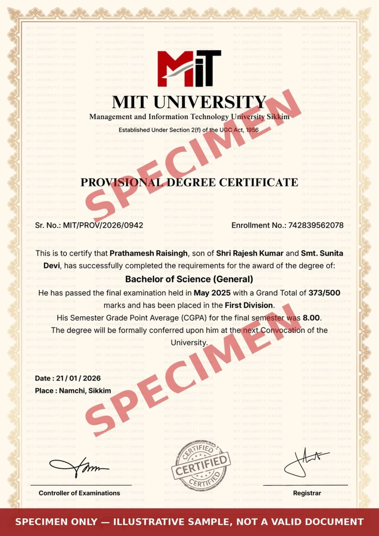
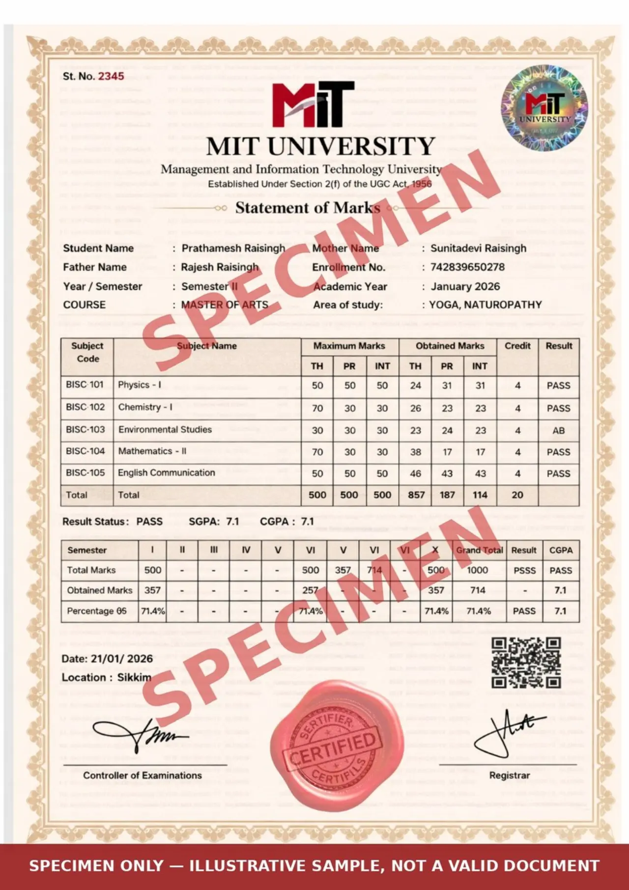
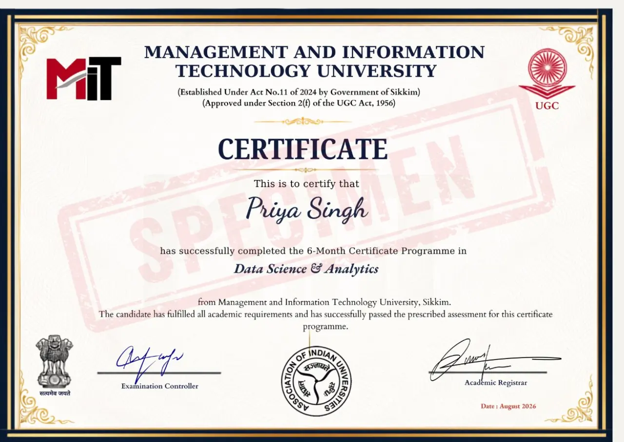
On completing the MTech in Electronics & Communication (VLSI Design / Communication System) programme at MIT University Sikkim, students receive official, verifiable documents. Specimen samples are shown below — names, marks and dates are fictitious and the images are watermarked; they are invalid for any official use.

Sample provisional degree certificate of MIT University Sikkim

Provisional Degree Certificate

Issued after successful completion of the programme, bearing the university seal and signatures.

Sample statement of marks (marksheet) of MIT University Sikkim

Statement of Marks

Semester-wise marksheet showing subjects, credits and grades under the CBCS / NEP 2020 framework.

Sample certificate issued for a certificate programme

Programme Certificate

Landscape certificate awarded on completion of certificate and diploma programmes.

Specimen only — these samples cannot be used as proof of education. Original documents are issued solely by the university's examination division.

View All Samples
Verified & Authentic

University Recognition Documents

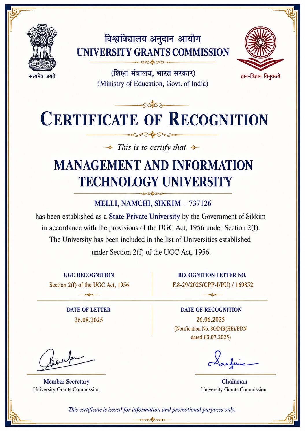
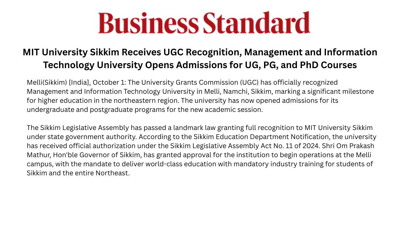
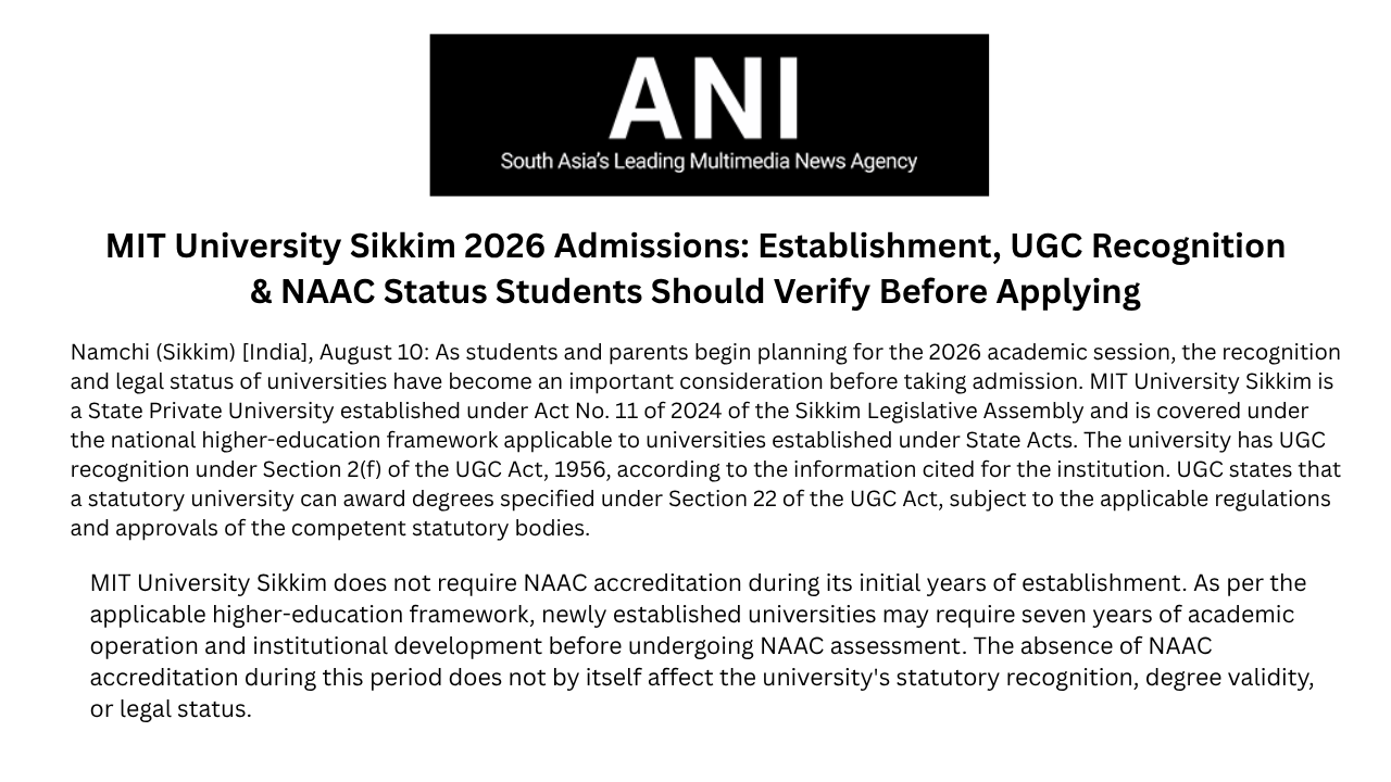
Your MTech in Electronics & Communication (VLSI Design / Communication System) degree is backed by these official recognitions. Below are the actual recognition documents issued to MIT University Sikkim.

UGC Certificate of Recognition for Management and Information Technology University, Sikkim

UGC Certificate of Recognition

Established as a State Private University by the Government of Sikkim under Section 2(f) of the UGC Act, 1956.

View UGC Letter (PDF)
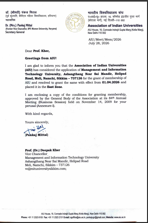
Association of Indian Universities membership grant letter dated July 28, 2026

AIU Membership Letter

Association of Indian Universities (AIU) membership granted with effect from 01.04.2026, East Zone.

View AIU Letter
Degrees awarded by MIT University Sikkim are valid for higher studies, government jobs and employment in India and abroad.
Degree Validity & Verification

FAQs: Is the Degree Valid?